What Can ABACUS Do Too? | Explain the Formation Mechanism of Conductive Filaments in RRAM Based on TiOx/MoS2–xOx Structure Induced by S Vacancies
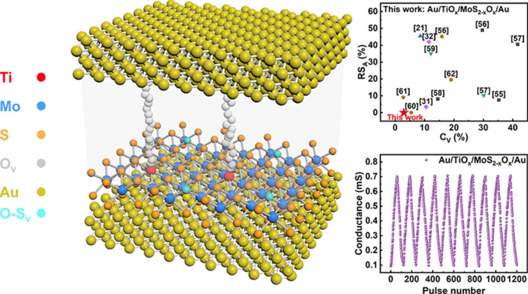
Recently, the experimental team led by Yuanyuan Shi from the University of Science and Technology of China collaborated with the theoretical team from the Hefei Comprehensive National Science Center Institute of Artificial Intelligence. They controlled the formation of conductive filaments by using a single layer of MoS₂ as an interlayer in the TiOₓ resistive switching layer of analog resistive random access memory (analog RRAM). This improved the device's switching uniformity, linearity, and symmetry. The voltage difference between switching cycles was only 1.28% and 1.7%. This structure also achieved high conductance modulation linearity and 64 conductance states (6-bit), and the on-chip training accuracy was as high as 93.02%. The researchers used the domestic open-source density functional theory software ABACUS (Atomic Abacus) to calculate the diffusion, migration, and defect structures of Ti ions on the MoS₂ surface and successfully explained the formation mechanism of conductive filaments in RRAM based on the TiOₓ/MoS₂–xOₓ structure induced by S vacancies. This work effectively improved the uniformity, linearity, and symmetry of analog RRAM devices and provided an impetus for the development of RRAM-based in-memory computing chips. The research results "Uniformity, Linearity, and Symmetry Enhancement in TiOₓ/MoS₂–xOₓ Based Analog RRAM via S-Vacancy Confined Nanofilament" have been published in the Nano Letters journal (Nano Lett. 24, 51, 16283–16292 (2024)).
Paper link: https://pubs.acs.org/doi/10.1021/acs.nanolett.4c04434
Research Background
Analog RRAM is widely used in in-memory computing chips due to its advantages in multi-level conductance states, good retention, and durability. However, simultaneously achieving low variability, high linearity, and symmetry in conductance adjustment remains a challenge, which limits their potential applications in edge computing or continuous learning. The resistive switching mechanism of traditional oxide-based RRAM is widely believed to be caused by the formation/rupture of conductive filaments due to the generation/dissolution of oxygen vacancies. Due to the inherent random generation/dissolution of oxygen vacancies under the influence of electric fields and thermal effects, the conductive filaments are usually network-like, resulting in large conductance changes, non-linearity, and asymmetry. The random formation of conductive filaments often makes it difficult to simultaneously achieve low variability, high linearity of conductance modulation, and symmetry, which complicates on-chip training and limits the application scenarios of RRAM-based in-memory computing chips.

Figure 1: Demonstration of the RRAM design scheme based on a single-layer MoS₂ interlayer adopted in this study, the benchmark diagram of the uniformity between cycles and the switching symmetry of the device, as well as the conductance modulation linearity of the analog RRAM used in this work.
Research Results
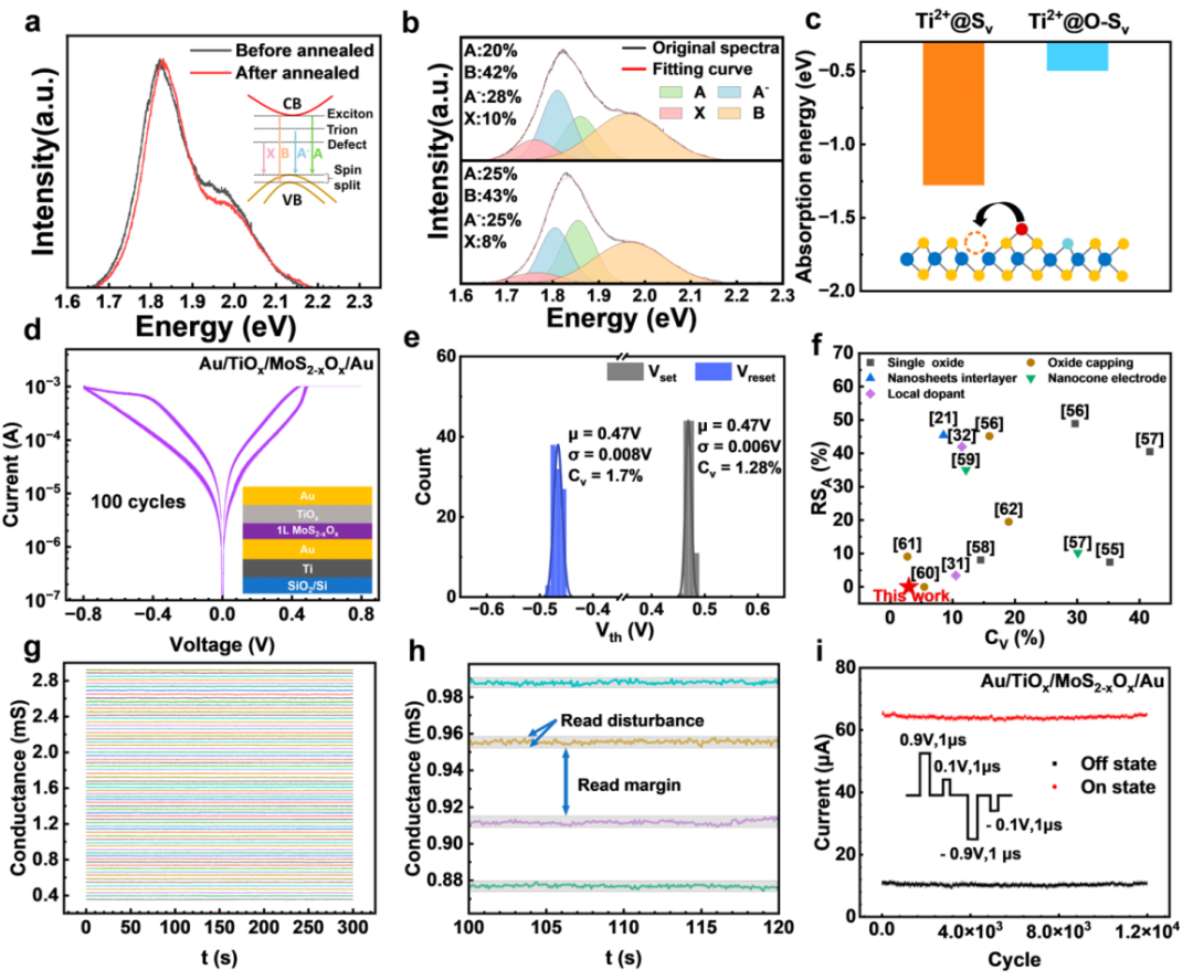
Yuanyuan Shi's experimental team proposed a simple and effective method to control the formation of conductive filaments by inserting a single layer of MoS₂ into the TiOₓ switching layer. Furthermore, by annealing MoS₂ in an air atmosphere, the limited sulfur vacancies (Sₓ) in the formed MoS₂−xOₓ interlayer can further limit the position, size, and number of conductive filaments, thus achieving highly uniform and symmetric switching behavior. In the TiOₓ/MoS₂−xOₓ-based RRAM, the Set voltage and Reset voltage are symmetric, with changes of only 1.28% and 1.7% during the cycle. In addition, high conductance modulation linearity and 64 conductance states were achieved, which contributed to an on-chip training accuracy of up to 93.02%.

Figure 2: Improvement of resistive switching uniformity and symmetry in Au/TiOₓ/MoS₂−xOₓ/Au.
Dr. Xudong Zhu from the theoretical calculation team used ABACUS first-principles calculations combined with the NEB method to analyze in detail the diffusion and adsorption behaviors of Ti atoms/ions on ML MoS₂. It was found that the diffusion energy barriers of Ti²⁺, Ti³⁺, and Ti⁴⁺ ions on the MoS₂ surface are 0.65 eV, 0.80 eV, and 0.88 eV, respectively, indicating that the spontaneous diffusion of these ions on the MoS₂ surface is relatively difficult. However, the adsorption energies of these ions at Sₓ are -1.28 eV, -0.61 eV, and -0.13 eV, respectively, showing a strong adsorption tendency. Especially for Ti²⁺ ions, not only is the adsorption energy at Sₓ the lowest, but also the diffusion energy barrier on the MoS₂ surface is the lowest, making Ti²⁺ ions a key factor in the formation of conductive filaments.

Figure 3: The role of a single layer of MoS₂ in the formation of conductive filaments. (a) The I-V curve of Au/TiOₓ/MoS₂/Au RRAM was fitted using the Schottky emission model. The inset shows the Schottky barrier formed at the Au/MoS₂ interface. (b) The diffusion and adsorption energies of Ti atoms/ions on a single layer of MoS₂. (c) The density of states of MoS₂ with Sₓ defects and the adsorption of Ti atoms/ions on sulfur vacancies. (d-f) Schematic diagrams of the formation of conductive filaments restricted by Sₓ in Au/TiOₓ/MoS₂/Au RRAM.
Through the calculation of the electronic structure, the position of the defect energy level introduced by the S vacancy in the MoS₂ bandgap and the change of the energy level after Ti ion adsorption were further revealed. For neutral Ti atoms, MoS₂ remains a semiconductor after adsorption; while for Ti²⁺, Ti³⁺, and Ti⁴⁺ ions, the Eₓ of MoS₂ enters the valence band after adsorption, indicating that MoS₂ becomes a conductive state. This shows that the adsorption of all charged Ti ions causes the single-layer MoS₂ to change from a semiconductor state to a conductive state. These local conductive sites limit the position, size, and number of conductive filaments, thereby improving the uniformity, linearity, and symmetry of the device.
Outlook
The MoS₂ interlayer proposed in this study solved the problems of variability, non-linearity, and asymmetry in RRAM caused by the random formation of conductive filaments. By combining experimental and theoretical calculations, the physical mechanism for improving device uniformity was elucidated, providing new ideas for future performance improvement of RRAM devices. With the wide application of computing memory chips, how to ensure that RRAM remains efficient and stable in a wider working environment (such as extreme temperatures and long-term operation) will also become a future research focus. In addition, combined with on-chip training technologies of deep learning and machine learning, how to further improve the application performance of RRAM in intelligent computing will be another frontier direction of future research. This work not only provides a new way for RRAM performance optimization but also provides a corresponding research foundation for developing high-performance, low-power consumption, and low-variability RRAM chips.
Acknowledgments
Dongdong Sun, a doctoral student at the University of Science and Technology of China, and Xudong Zhu, a postdoctoral researcher at the Hefei Comprehensive National Science Center Institute of Artificial Intelligence, are the co-first authors of this paper. Yuanyuan Shi and Lixin He, professors at the University of Science and Technology of China, and Shaochuan Chen, a doctor from RWTH Aachen University, are the co-corresponding authors. This research was funded by the National Natural Science Foundation of China, the China Postdoctoral Science Foundation, and the Anhui Postdoctoral Fund. It also received support from the Micro and Nano Research and Manufacturing Center, the Physical and Chemical Center, and the Supercomputing Center of the University of Science and Technology of China.
Related Links
ABACUS official website:
https://abacus.deepmodeling.com
Py-ATB software:
https://github.com/pyatb
ATST-Tools project:
https://github.com/QuantumMisaka/ATST-Tools